Laboratory-Grown Diamonds, engineered for impact Enhancing today’s systems and enabling tomorrow’s devices
Laboratory-Grown Diamonds, engineered for impact Enhancing today’s systems and enabling tomorrow’s devices
Transforming industries through advanced diamond technology
KGK Diamatrix engineers Laboratory-Grown Diamonds as an advanced material, reshaping the foundations of performance across technologies. As part of the KGK Group, we combine operational efficiency with the power to deliver breakthrough innovations on a global scale. We enhance today’s technologies and unlock tomorrow’s devices - transforming industries and defining the material stack of the future.

Diamond materials for thermal solutions
and diamond-based devices.

NV-diamond for quantum sensing with pathways
to computing and communication.

Nanocrystalline coatings for optical,
biomedical, and industrial use.

Single-crystal and polycrystalline tools
for precision machining.
Across forms, properties, and formats, we engineer diamond for performance.
Designed for purpose - we tune properties and build to spec.
From selection to production, we integrate diamond into working systems at scale.
Across forms, properties, and formats, we engineer diamond for performance.
Designed for purpose - we tune properties and build to spec.

From selection to production, we integrate diamond into working systems at scale.
Precision-engineered diamond materials for next-generation applications

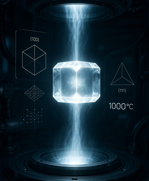
High-purity single-crystal diamond engineered for semiconductor platforms—combining high thermal conductivity and high dielectric strength. Supplied undoped or boron-doped for use as substrates, interlayers, or as an active semiconductor material.
Contact Us for Product Specifications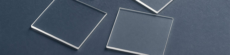
Single-crystal diamond plates purpose-built for heat spreading and electrical isolation in power, RF, and other electronic applications. Optional metallization available; high thermal conductivity and tight flatness support higher power density and reliability.
Contact Us for Product Specifications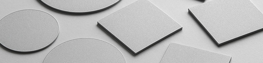
Polycrystalline diamond wafers and plates for large-area thermal management. Available freestanding or on a silicon base, offering high in-plane conductivity and mechanical robustness.
Contact Us for Product Specifications
High-purity single-crystal diamond for quantum applications, available with 12C isotopic enrichment. Low-defect, low-strain material suitable for further processing.
Contact Us for Product Specifications
Diamond plates with controlled, uniform bulk NV concentration for ensemble magnetometry and imaging. Engineered for consistent signal performance across the active area. Available with 12C isotopic enrichment.
Contact Us for Product Specifications
Near-surface NV diamond with precise depth control and tailored surface preparation for nanoscale magnetometry and scanning-probe sensing. Available with 12C isotopic enrichment.
Contact Us for Product Specifications
Nanocrystalline diamond coatings applied to customer substrates to extend wear life, reduce friction, and improve thermal performance. Chemically inert and biocompatible films tailored in thickness for optical, biomedical, and industrial needs.
Contact Us for Product Specifications
Single-crystal diamond turning tools for ultra-precision machining of non-ferrous metals, polymers, and optical materials. Extremely sharp edges deliver mirror-finish surfaces, tight tolerances, and long tool life.
Contact Us for Product SpecificationsReady to explore how KGK Diamatrix
can advance your technology? Get in
touch with our team.

 info@kgkdiamatrix.com